
Understanding electronic schematics, often found in PDF format, is crucial for anyone involved in electronics design,
troubleshooting, or modification. These diagrams represent the components and connections within a circuit,
providing a blueprint for functionality and enabling effective analysis of complex systems. Altium 365 offers
cloud-based viewing, while resources like Stan Gibilisco’s guide aid comprehension.
What is an Electronic Schematic?
An electronic schematic, fundamentally, is a visual representation of an electronic circuit. Unlike a physical layout showing component placement, a schematic focuses on the functionality and connections between components. It employs standardized symbols – resistors, capacitors, transistors, and more – to illustrate these elements and their interrelationships. These diagrams are essential for engineers, technicians, and hobbyists alike, serving as a roadmap for building, analyzing, and repairing electronic devices.
Typically encountered as PDF documents, schematics abstract away physical details, prioritizing logical flow. They depict how electricity travels through the circuit, highlighting key signal paths and power distribution. Understanding these symbols and their connections is paramount. Resources like beginner’s guides, such as those by Stan Gibilisco, are invaluable for deciphering these visual languages. Schematics aren’t merely pictures; they are precise technical drawings conveying critical information about a circuit’s operation.
Why Read Electronic Schematics?
The ability to read electronic schematics is indispensable for anyone working with electronics. It’s crucial for troubleshooting malfunctioning circuits, allowing you to pinpoint faulty components and understand signal flow. Schematics are also vital for designing new circuits, providing a clear framework for component selection and interconnection. Furthermore, understanding schematics enables effective modification of existing designs, facilitating upgrades or customizations.
Without schematic literacy, reverse engineering a device or understanding its operational principles becomes significantly harder. Tools like Altium 365 Viewer allow for easy visualization and cross-probing of schematics within PDF documents. Mastering schematic reading unlocks a deeper understanding of electronics, empowering you to analyze, repair, and innovate. It’s a foundational skill for electrical engineers, technicians, and serious hobbyists, bridging the gap between theory and practice.
Understanding Schematic Symbols
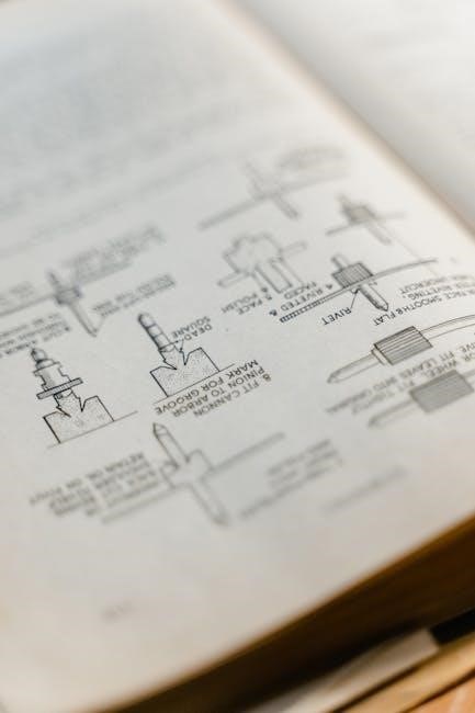
Decoding schematic symbols—resistors, capacitors, transistors, and diodes—is fundamental. Recognizing these graphical representations unlocks circuit comprehension, enabling effective analysis and design.
Resistors and Their Symbols
Resistors, fundamental components limiting current flow, are represented in schematics by several standardized symbols. The most common is a zig-zag line, denoting resistance without specifying a value. American and European standards differ slightly; the American symbol resembles a rectangular block with the zig-zag, while the European version is a simple zig-zag.
Understanding resistor symbols is paramount for tracing current paths and calculating voltage drops within a circuit. Schematics often indicate resistance value using numerical codes alongside the symbol, employing Ohm’s Law (V=IR) for calculations; Potentiometers, variable resistors, are shown with an adjustable arrow through the zig-zag line. PDF viewers, like Altium 365, facilitate zooming to clearly discern these details. Properly interpreting these symbols is a cornerstone of schematic reading, enabling accurate circuit analysis and troubleshooting.
Capacitors and Their Symbols
Capacitors, storing electrical energy in an electric field, are depicted with two parallel lines in schematic diagrams. These lines symbolize the capacitor’s plates. The key distinction lies in whether the symbol indicates a polarized or non-polarized capacitor. Non-polarized capacitors, commonly ceramic or film types, have identical parallel lines.
Polarized capacitors, like electrolytic or tantalum types, require correct orientation; their symbol features a curved line representing the negative terminal. Incorrect polarity can lead to damage or failure. PDF schematic viewers, with zoom capabilities, are essential for verifying polarity markings. Capacitance value is usually indicated near the symbol, often in Farads (F), microfarads (µF), or picofarads (pF). Mastering capacitor symbols and recognizing polarity is vital for accurate circuit interpretation and safe electronic work, especially when using tools like OrCAD.
Inductors and Their Symbols
Inductors, components storing energy in a magnetic field, are represented in schematics by a coiled wire symbol. This symbol visually depicts the winding of the inductor. Variations exist to indicate different types and characteristics. An inductor with a core, such as ferrite, may have parallel lines within the coil symbol to signify the core material.
The inductance value, measured in Henries (H), millihenries (mH), or microhenries (µH), is typically noted near the symbol. PDF viewers with cross-probing features allow tracing connections to associated components. Understanding the symbol variations helps differentiate between air-core and core-based inductors. Accurate interpretation is crucial for analyzing circuits involving resonant frequencies or filtering. Utilizing software like Altium 365 can enhance visualization and comprehension of complex inductor arrangements within a schematic PDF.

Diodes and Their Symbols
Diodes, fundamental semiconductor devices allowing current flow in one direction, are represented by a triangle pointing towards a vertical line in schematics. The triangle signifies the anode (positive terminal), while the line represents the cathode (negative terminal). Variations exist, such as a circle at the tip of the triangle, indicating a Schottky diode.
PDF schematic viewers, like those offered by Altium 365, facilitate zooming and detailed inspection of these symbols. Understanding the diode’s polarity is critical for correct circuit analysis. The symbol’s orientation indicates the direction of current flow. Resources like beginner’s guides emphasize recognizing these symbols quickly. Identifying diodes within a PDF schematic allows tracing signal paths and understanding rectification or switching circuits. Proper interpretation is essential for troubleshooting and design verification.
Transistors and Their Symbols
Transistors, crucial for amplification and switching, present more complex symbols than diodes. Bipolar Junction Transistors (BJTs) have variations depending on NPN or PNP type. NPN transistors feature an arrow pointing out of the base, while PNP transistors have an arrow pointing in. Field-Effect Transistors (FETs) utilize a different symbol, with a line representing the gate, and an arrow indicating the channel direction.
When viewing PDF schematics, utilizing features like zoom within Altium 365 or similar viewers is vital for discerning these subtle differences. Correctly identifying transistor types is paramount for understanding circuit behavior. Beginner’s guides, such as those by Stan Gibilisco, provide detailed symbol explanations. Recognizing these symbols enables tracing signal paths and analyzing amplifier stages or switching circuits within the PDF document.

Navigating PDF Schematic Documents
Effectively navigating PDFs requires utilizing viewer features like zoom and search. Altium 365 facilitates cross-probing and layer management, enhancing schematic comprehension and analysis.
Using PDF Viewer Features (Zoom, Search)
Mastering PDF viewer features is paramount when dissecting electronic schematics. Zoom functionality allows for detailed inspection of intricate component arrangements and trace connections, crucial for identifying subtle design elements. Utilize the search capability to quickly locate specific components, reference designators, or net names within the schematic document. This is particularly helpful in large, complex schematics where manual searching would be incredibly time-consuming.
Many PDF viewers offer advanced features like bookmarks and thumbnails, enabling rapid navigation between different sections of the schematic. Furthermore, tools for measuring distances and angles can be invaluable for verifying component placement and trace lengths. Experiment with different viewer settings to optimize the display for clarity and readability, adjusting brightness, contrast, and color schemes as needed. Remember that effective use of these features significantly streamlines the schematic interpretation process;
Layer Management in Schematics
Modern electronic schematics often employ layers to organize information, and understanding this is vital for effective reading. Different layers might represent power distribution, signal routing, component placement, or mechanical details. PDF viewers with layer management capabilities allow you to selectively display or hide these layers, simplifying the schematic for focused analysis. For instance, isolating the power layer helps identify voltage rails and ground connections quickly.
Being able to toggle layer visibility prevents visual clutter and allows you to concentrate on specific aspects of the design. Some schematics utilize layers to denote different schematic sheets or revisions. Familiarize yourself with the layer naming conventions used in the specific schematic you are examining. Proper layer management is essential for navigating complex designs and extracting meaningful information efficiently, enhancing comprehension and reducing errors.
Cross-Probing and Netlist Exploration
Advanced PDF schematic viewers, like Altium 365, offer powerful features such as cross-probing. This allows you to click on a component in the schematic and instantly highlight its connections on the PCB layout, or vice versa. This bidirectional link significantly speeds up debugging and understanding the physical implementation of the circuit. Netlist exploration is another crucial technique. A netlist is a textual description of all the connections in the schematic.
Examining the netlist can help identify signal paths, locate short circuits, or verify connectivity. Some tools allow you to search the netlist for specific components or nets. Utilizing these features, alongside the schematic itself, provides a comprehensive understanding of the circuit’s behavior. Effectively leveraging cross-probing and netlist exploration dramatically improves the efficiency of schematic analysis and troubleshooting.

Software Tools for Schematic Viewing
Various software options facilitate schematic viewing, including Altium 365, OrCAD, and general PDF editors with markup capabilities, enhancing PDF schematic interpretation.
Altium 365 Viewer
Altium 365 provides a powerful, cloud-based solution for visualizing and sharing electronic design projects, including schematic documents in PDF and other formats. This viewer allows users to upload schematic, PCB, and complete project archives for convenient access from any device with an internet connection. A key feature is the ability to freely cross-probe between schematic, PCB, and 3D views, enabling a comprehensive understanding of the design.
Furthermore, Altium 365 offers access to the Bill of Materials (BOM) and component pricing information directly within the viewer, streamlining the procurement process. Its intuitive interface and collaborative features make it ideal for teams working on complex electronic designs. The platform supports various file formats, ensuring compatibility with a wide range of projects, and eliminates the need for specialized software installations, simplifying the viewing experience for stakeholders.
OrCAD Schematic Editor
OrCAD, a widely recognized name in PCB design, historically served as a primary tool for drafting electronic schematics. While primarily a schematic editor for creation and modification, its capabilities extend to viewing and interpreting existing schematics, including those exported as PDFs. Experienced electrical engineers often utilized OrCAD during their PCB design workflows, becoming proficient in its interface and features.
Though not strictly a PDF viewer, OrCAD allows for opening and analyzing schematic files directly, providing detailed component information and connectivity data. This direct access facilitates a deeper understanding of the circuit’s functionality compared to simply viewing a static PDF. Its robust features enable tracing signal paths and identifying potential design issues, making it a valuable tool for both novice and experienced engineers when dealing with complex electronic schematics.

General Purpose PDF Editors with Markup Tools
While specialized software excels, general-purpose PDF editors equipped with markup tools offer a practical approach to reading and interpreting electronic schematics in PDF format. These editors, available on all platforms, allow for zooming, panning, and adding annotations directly onto the schematic diagram. This functionality is invaluable for highlighting key components, tracing signal paths, or noting potential issues during review.
Features like real-time collaboration and commenting facilitate teamwork and knowledge sharing. Intuitive tools enable users to draw shapes, add text, and measure distances, aiding in the analysis of component placement and circuit layout. Though lacking the advanced features of dedicated schematic viewers like Altium 365, these editors provide a versatile and accessible solution for basic schematic interpretation and documentation.

Advanced Techniques

Mastering schematic reading involves tracing signal paths, identifying crucial ground and power rails, and deciphering complex bus structures for efficient circuit analysis.
Tracing Signal Paths
Effectively tracing signal paths within a schematic is a fundamental skill. Begin by identifying the source of a signal and meticulously follow its journey through the circuit. Utilize PDF viewer features like zoom to closely examine connections and component pins. Cross-probing, available in tools like Altium 365 Viewer, allows you to instantly jump between schematic symbols and their corresponding PCB layout, aiding in path verification.

Pay close attention to net names – labels assigned to conductive tracks – as they provide valuable clues. Look for changes in net names, indicating signal transformations or branching. Be mindful of hierarchical schematics, where sections of the circuit are represented as blocks; you may need to drill down into sub-sheets to fully trace the path. Careful observation and systematic tracking are key to understanding signal flow and diagnosing potential issues.
Identifying Ground and Power Rails
Recognizing ground and power rails is essential for schematic interpretation. These rails, typically represented by horizontal lines, distribute power and provide a common reference point for signals. Ground is often denoted by symbols resembling stacked lines or a triangle, while power rails are labeled with voltage values (e.g., +5V, +12V, -3.3V).
PDF viewers with markup tools can be used to highlight these rails for clarity. Pay attention to how components connect to these rails; this reveals their power supply and grounding scheme. Understanding the power distribution network is crucial for troubleshooting and ensuring circuit stability. Look for decoupling capacitors placed near integrated circuits – these minimize noise and provide a local energy reservoir. Careful identification of these rails provides a foundational understanding of the circuit’s operation.
Understanding Bus Structures
Bus structures in schematics represent groups of signals that share common pathways, simplifying complex interconnections. These are often depicted as a collection of parallel lines, each representing a separate signal – like address, data, or control lines. Identifying bus structures is vital for understanding data flow within a system.
PDF schematic viewers with cross-probing capabilities allow tracing signals within a bus to their source and destination. Look for labels indicating the bus’s function (e.g., “Address Bus,” “Data Bus”). Understanding the bit-width of a bus (e.g., 8-bit, 16-bit) reveals the amount of data it can transmit simultaneously. Recognizing bus structures streamlines schematic analysis, enabling efficient comprehension of complex digital circuits and their interactions.

Resources for Learning
Explore beginner guides like Stan Gibilisco’s book and engage with online forums for collaborative learning. Utilize the Internet Archive and Altium’s resources.
Beginner’s Guides (Stan Gibilisco’s Book)
Stan Gibilisco’s “Beginner’s Guide to Reading Schematics” (3rd Edition), available through the Internet Archive (PDFDrive.com), is a highly recommended starting point for novices. This comprehensive resource systematically introduces schematic symbols, circuit analysis techniques, and practical applications. It breaks down complex concepts into digestible segments, making it accessible to individuals with limited prior knowledge.
The book emphasizes a step-by-step approach to deciphering schematics, covering essential topics like resistors, capacitors, inductors, diodes, and transistors. Gibilisco’s guide doesn’t just present symbols; it explains their function within a circuit and how to trace signal paths. It’s a valuable tool for building a solid foundation in electronic schematic interpretation, enabling readers to confidently navigate and understand electronic designs. The availability of a PDF version enhances accessibility and allows for convenient study and reference.
Online Forums and Communities
Engaging with online forums and communities dedicated to electronics is an invaluable supplement to formal learning resources when mastering schematic interpretation. These platforms provide a space to ask questions, share knowledge, and learn from experienced hobbyists and professionals. Seeking clarification on specific symbols, circuit behaviors, or PDF navigation challenges becomes readily achievable through collaborative discussion.
Numerous online communities offer dedicated threads for schematic reading assistance, fostering a supportive learning environment. Sharing schematics for review and receiving constructive feedback can accelerate understanding. Furthermore, these forums often host discussions on software tools like Altium 365 Viewer and OrCAD, providing practical insights into utilizing these resources effectively. Active participation in these communities transforms learning from a solitary pursuit into a dynamic, interactive experience, enhancing comprehension and problem-solving skills.
Further Reading on Electronic Components
Deepening your understanding of individual electronic components is paramount to effectively interpreting schematics. While schematics illustrate connections, knowing the function and characteristics of each component – resistors, capacitors, transistors, diodes, and inductors – unlocks true comprehension. Resources beyond basic schematic guides are essential for this.
Exploring datasheets for specific components reveals critical parameters like voltage ratings, tolerances, and power dissipation. Books like Stan Gibilisco’s guide provide foundational knowledge, but supplementing this with component-specific literature is crucial. Understanding how components interact within a circuit, informed by their individual properties, allows for accurate analysis of schematic diagrams. This knowledge empowers you to predict circuit behavior and troubleshoot effectively, especially when utilizing PDF schematics viewed with tools like Altium 365.